Among other things, it was possible to grow novel isolator crystals using lasers. The project, funded with €6.22 million by the Federal Ministry for Research, Technology and Space (BMFTR), has made further significant progress during the runtime from November 2021 to July 2025. Fraunhofer ILT in Aachen has made a significant contribution.
Still, beam sources for quantum technology applications are often complex, large, and not robust enough for field use. There is a need for miniaturized and as flexible as possible systems. Such a beam source has been developed in the BMFTR-funded project 'HiPEQ – Highly integrated PIC-based ECDLs for quantum technology'. Coordinated by the later system integrator TOPTICA, a consortium of industry and research has built demonstrators of two miniaturized beam sources.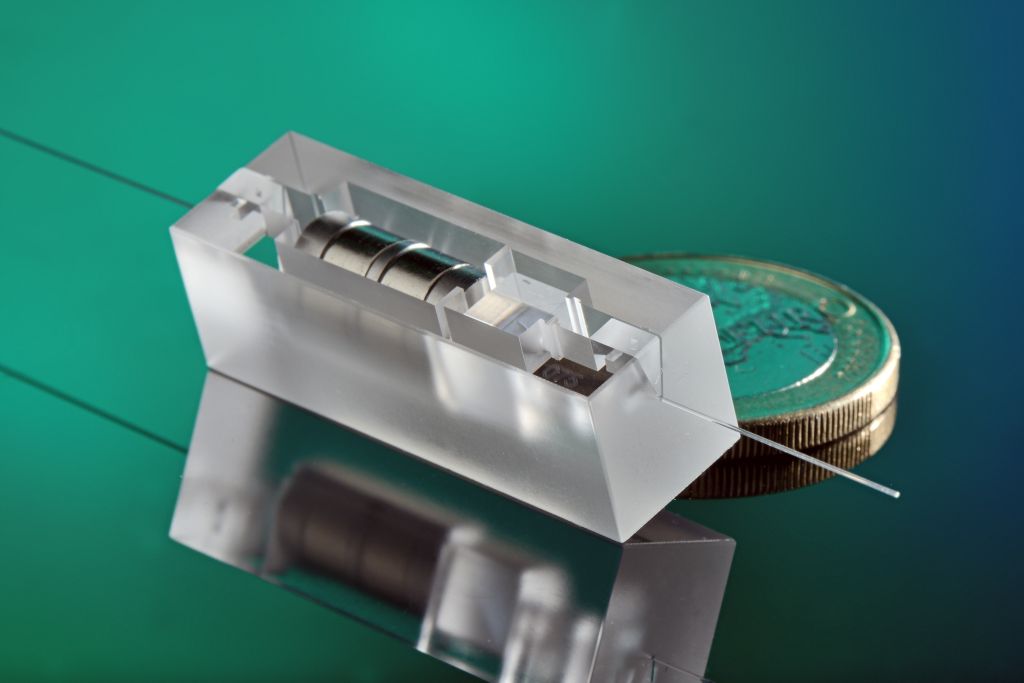
With an external dimension of only 22 x 9 x 6 cm³, they provide space for all system components. The concept is also expandable to other wavelengths. They can therefore be used in a wide range of quantum technology applications.
Fraunhofer ILT was able to significantly contribute to the successful growth of previously unavailable crystals for novel Faraday isolators in the project. In a second work package, the Aachen team realized a glass packaging module with μm-precise mounts for important system components and for fiber coupling.
Compact, robust, and flexible to use
The laser systems are based on photonic integrated circuits (PICs), optical fibers, a fiber coupling, and an optical isolator that shields reflections of the radiation in the laser. This key component is based on special crystals that exhibit the magneto-optical Faraday effect: When a magnetic field is applied, the polarization plane of incoming light waves rotates in the crystal. Through this Faraday rotation, reflected light – if at all – can then only return to the beam source extremely damped. In this way, isolators prevent damage and ensure the narrowband nature of the lasers, which is essential for quantum technology applications.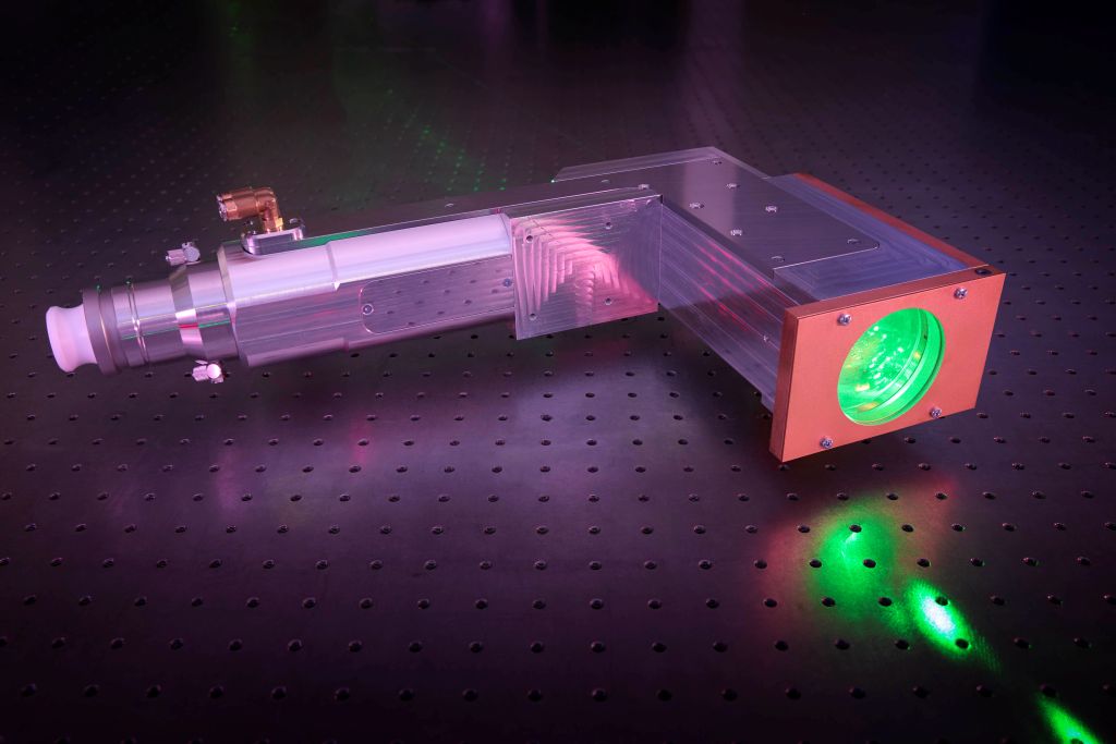
So far, Faraday isolators have mostly been based on terbium-gallium garnet (TGG), which has a high Verdet constant for visible and near-infrared light; this indicates the strength of the Faraday effect. 'TGG isolators typically have a length of about 25 millimeters,' reports Florian Rackerseder, the project manager at Fraunhofer ILT. For miniaturization, crystals with a higher Verdet constant are needed, which provide shielding in less space. These crystals for Faraday isolators have been grown and tested in the HiPEQ project.
The choice fell on a material based on the naturally occurring terbium (III) oxide (Tb2O3).
It has a three times higher Verdet constant than TGG and is particularly suitable for lasers in the blue wavelength range, for which there was previously no suitable material. 'Growing Tb2O3 monocrystalline is a challenge,' explains the expert, 'because at melting temperatures beyond 2,500 °C, precise temperature gradients must be maintained during the transition to the stable phase.' This refers to the transition from the molten ceramic starting material to the Tb2O3 crystal. The cooling rates are crucial for the quality of the crystal; the process is so sensitive that conventional methods of crystal growth have never succeeded in producing Tb2O3 in the size and quality required for isolators. To stabilize the cubic phase in which the material is grown and thus simplify the growth process, co-doping with lutetium oxide (Lu2O3) was used.
Laser technology as a key for growing high-purity crystals
In a HiPEQ subproject, SurfaceNet, Laserline, and Fraunhofer ILT developed and realized a new facility where (TbxLu1-x)2O3 isolator crystals grow in the so-called laser-based optical floating zone process (LOFZ). The transition from the molten ceramic to the crystal occurs at the edge of the floating zone, which is directed by four processing optics. These direct the radiation from four diode lasers, each with a maximum optical power of 3 kW, onto the ceramic feed rod and melt it into a single crystal.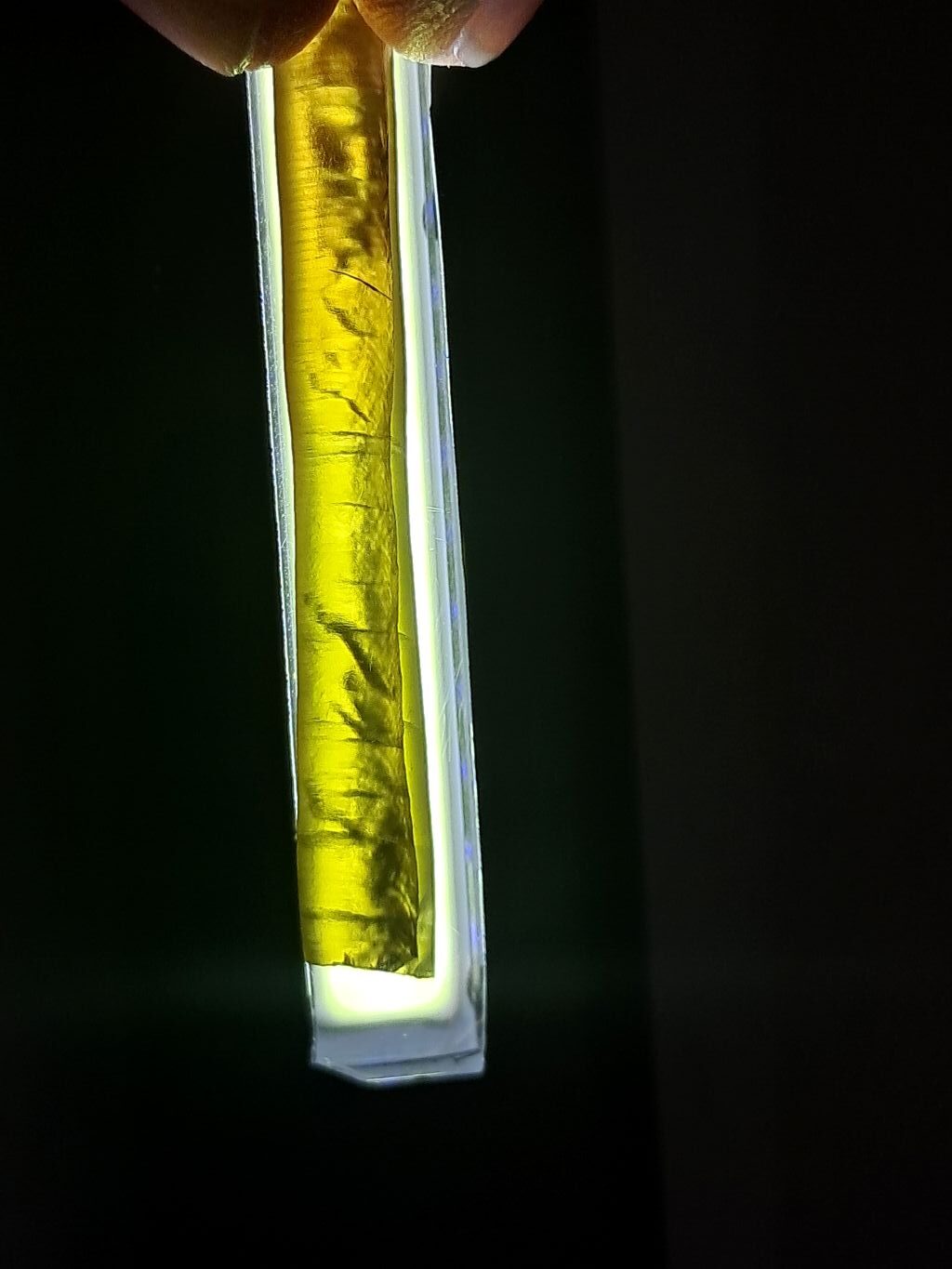
The irradiation optimized in simulations with trapezoidal, extremely homogeneous beam profiles ensures uniform heating power densities in the floating zone. The intensity distribution in the focus can be adjusted by modifications in the beam path. 'The trapezoidal geometry has the advantage that a large part of the introduced laser energy melts the ceramic, and the rest regulates the temperature during solidification into the crystal,' explains Rackerseder. In the continuous remelting process with constant feed speed, the crystal must leave the temperature range near the melting point only with precisely specified cooling rates. The team was able to meet this requirement using the precisely controlled LOFZ process. 'We are thus able for the first time to produce (TbxLu1-x)2O3 isolator crystals in the required size and quality,' he explains.
Fully integrated system
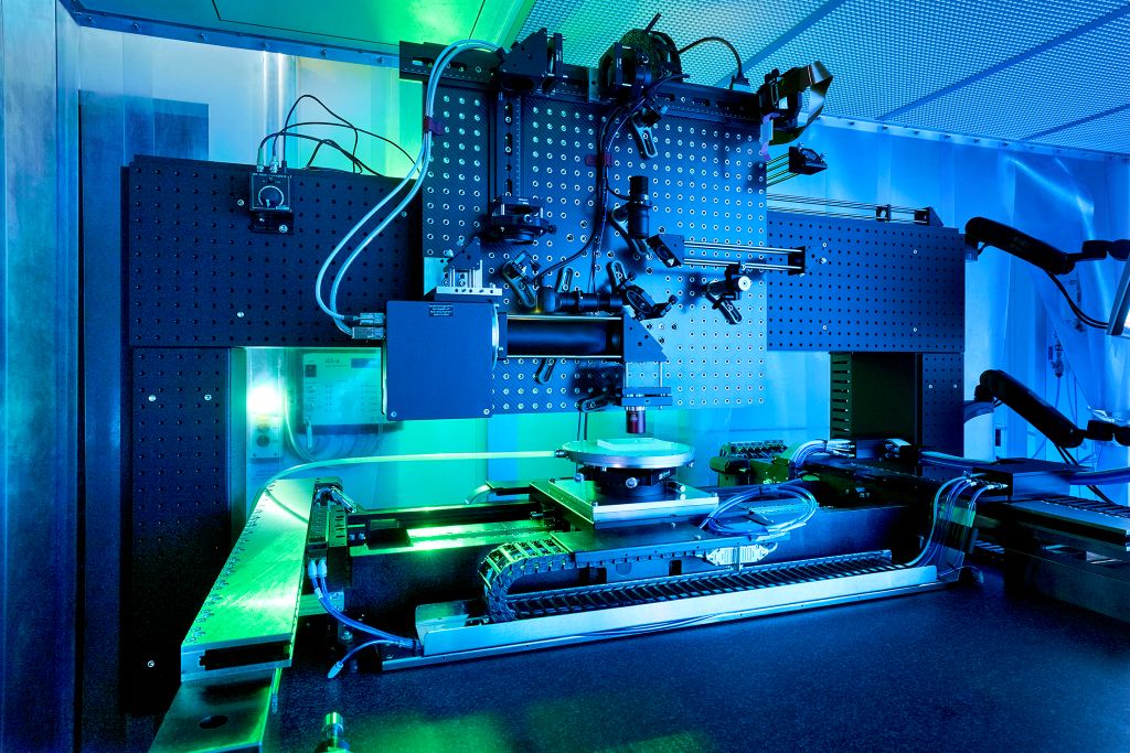
The new isolator crystals have been integrated by the HiPEQ consortium into modular miniaturized beam sources in another subproject. Fraunhofer ILT has also made a significant contribution to this. It has constructed a fiber-chip coupler that can be individually adapted to various system designs and made it from glass. The necessary flexibility and precision were achieved by the Selective Laser Induced Etching (SLE): A laser exposes microstructures in glass, which can then be precisely etched out. This allows for the realization of complex-shaped cavities inside the glass. In the project, this individual shaping of the SLE process was the key to being able to manufacture both beam sources monolithically at wavelengths of 461 nm (blue) and 637 nm (red), even though components of different dimensions are installed. The Faraday isolator is integrated just as precisely as the interface from the PIC to the optical fibers, which can be flexibly designed for the respective fiber diameters, including input and output optics and beam splitters. The SLE process ensures the μm-precise fitting of the respective different modules of both demonstrators.
"The fact that the surrounding material has the same thermal expansion coefficient as the optical components makes the fiber-chip coupler more robust against temperature fluctuations," explains Sandra Borzek, the person responsible for this part of the project at Fraunhofer ILT. Given the high precision requirements, stresses due to differing material expansion are unacceptable. And there was another driver for the project approach: "So far, the laser beam sources for quantum technologies are mostly adjusted manually," she explains. Each component, from the optics to the isolators and beam splitters to the fibers with single-digit µm diameters, is individually used and aligned.
The goal: Minimized adjustment and assembly effort
Photonics is looking for solutions that minimize assembly and adjustment effort while largely maintaining the required precision automatically. The packaging module, manufactured monolithically in a single SLE process, is already close to achieving this. Ideally, after being populated with the optical components, it serves as a fixed assembly that can be connected to the PIC using the so-called flip-chip bonding.
Originally, the SLE team wanted to manufacture the optics for coupling in and out of light in the SLE process and polish them with a laser. However, polishing the lenses in the component was impossible, and their surface was too rough after the SLE process. "We therefore developed various approaches to eliminate artifacts and residual ripples on the surfaces. This has brought us significantly closer to the goal of integrated optics and their polishing," reports Borzek. The team decided to manufacture the optics in the SLE process without a fixed connection to the monolithic glass body. This allows them to be removed for polishing and then precisely reinserted where they were taken out.
HiPEQ has generated know-how for future beam sources
With the successful cultivation of (TbxLu1-x)2O3 isolator crystals, the optimized process strategy for SLE-based optics manufacturing, and the direct integration of microscopic coupling structures into the macroscopic housing, HiPEQ has achieved important milestones. The consortium has generated the necessary know-how to implement flexible system designs with various isolators with significantly reduced assembly and adjustment effort. "On this basis, the glass packaging modules for flexible system designs could in the future be manufactured with µm precision in the SLE process within days. The novel Faraday isolators are a key technology for further miniaturization," Borzek and Rackerseder are convinced. HiPEQ has thus made significant contributions to the robustness, versatility, and reduced adjustment effort of lasers for quantum technological applications.
Contact: