Wire bonding has established itself as the standard method for electrical contacting in assembly and connection technology for 70 years across a wide range of applications. This ranges from semiconductor technology, microelectronics, and optical components to automobiles, consumer products, MEMS, and industrial sensors, as well as specific tasks such as bonding battery cells for electromobility, power tools, and energy storage. "Fundamentally, wire bonding is divided into three major process groups. Two of these are thin wire processes, where depending on the application, wires made of gold, silver, aluminum, or copper with diameters ranging from 18 to 50 µm are processed. The third group involves thick wire bonding with wire diameters from 100 to 500 µm," specifies Stefan Schmitz, managing director of Bond-IQ GmbH. The consulting company in wire bonding technology is the initiator of the industry project Surf:Guide. The project aims to develop a guideline for cleanliness and the condition of bond surfaces, which serves as a basis for creating an industrially recognized international standard.
Cleanliness - a quality-determining factor
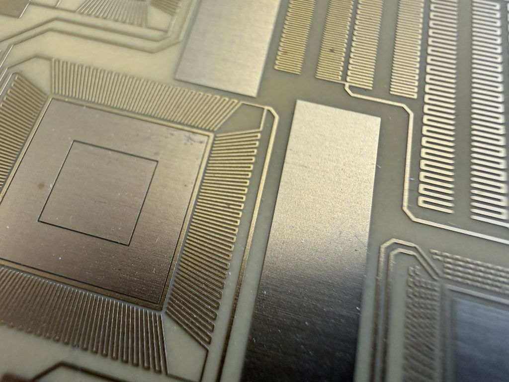
Since the formation of connections occurs in the nanometer range for both thin and thick wire bonding, the metals to be contacted must be brought to an atomic distance from each other. Accordingly, contaminants or intermediate layers as small as 5 to 10 nm can hinder the bonding process. These include, for example, fingerprints, bleeding adhesives, flux residues, outgassing from adhesives and other polymers, dust, oxides, or residues from particularly wet chemical cleaning processes.
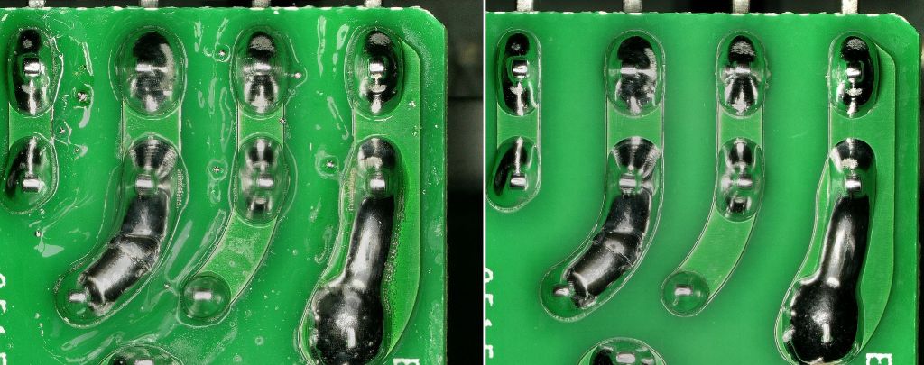
"Visibly detectable contaminations are critical for bonding. If these contaminants are no longer visible after cleaning, the bond surface is usually sufficiently clean. This can generally be determined with the help of a microscope and an optical before-and-after comparison. This alone can increase the success rate three to four times," explains Stefan Schmitz.
Methods for cleaning bond surfaces
Traditionally, bond surfaces are still cleaned using wet chemical processes with solvents or water-based media, which require energy-intensive drying. Plasma cleaning can be used for thin, known, and very specific contaminations. Another alternative is laser cleaning. "For very sensitive surfaces, such as in microelectronics, the costs for a laser system and the appropriate laser technology must first be aligned," describes Stefan Schmitz. "Currently, the industry's interest lies in the quattroClean snow jet cleaning, as it can also remove more strongly adhering, encrusted contaminants."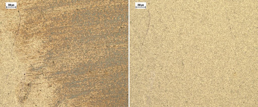
Dry, targeted, and sustainable cleaning
The scalable and cleanroom-capable quattroClean snow jet technology is a dry cleaning process for both large area and local applications. The process is suitable for reproducibly removing particulate contaminants down to the sub-micrometer range and filmic contaminations down to nanolayers. The quattroClean technology uses liquid, recycled carbon dioxide from chemical production processes and biomass energy generation as a cleaning medium. It is channeled through a flexibly adjustable, wear-free two-component ring nozzle and expands upon exit into fine snow crystals, which are bundled by a separate compressed air mantle jet and applied to the surface to be cleaned at supersonic speed. The cleaning effect is based on a combination of thermal, mechanical, solvent, and sublimation effects. Since the crystalline carbon dioxide completely sublimates during the process, the treated surfaces are dry. Removed contaminants are vacuumed away along with the process gas, preventing re-contamination of the surfaces and contamination of the environment. In combination with process gas from Linde, the effective quattroClean process has the Green Screen certificate for cleaners and degreasers from Clean Production Action.
Cleaning technology for a wide range of applications

The low hardness of the fine snow crystals allows for cleaning even very sensitive and finely structured surfaces. This opens up a very wide range of applications for the quattroClean snow jet technology. The process is used, among other things, for the removal of flux and solder residues on PCBs and PCBAs, the removal of chemical and particulate contaminants on bond pads, and the cleaning of battery cells before contacting. "On circuit boards, where there is often a mixture of organic residues such as fats, fingerprints, flux, or residues from wet chemical cleaning processes, the process can be used very efficiently. We have also achieved very good results on semiconductors and housings that come from galvanic or other wet chemical processes," reports Stefan Schmitz. The comparatively easy automation of the cleaning process or its integration into production lines also contributes to this.
"This results in two advantages. Automated cleaning ensures reproducibly homogeneous results. If cleaning is integrated into the manufacturing process, the freshly present contamination can be removed directly before it becomes an even bigger problem due to storage processes," adds Stefan Schmitz.
acp systems AG at Electronica in Hall A2, Stand 112.
Contact: