
At the 8th UKP Workshop on Ultrafast Laser Technology, 120 experts from 22 countries met on April 8 and 9 in Aachen. The name already suggests it: this workshop focuses on the generation and application of laser pulses in the range of picoseconds (ps) and femtoseconds (fs). These laser pulses can process practically any material. Research and development have made significant progress in recent years in the generation and application, so that this year's discussions mostly revolved around scaling the processes alongside new applications.
Scaling with more power and more wavelengths
Currently, industrial-grade laser beam sources with up to 1000 watts are available, for example from the system provider TRUMPF. This laser, with pulse energies of up to 10 mJ at pulse lengths under 1 ps, is available for testing at the Fraunhofer Cluster of Excellence Advanced Photon Sources CAPS application laboratory at Fraunhofer ILT or at TRUMPF itself in Schramberg.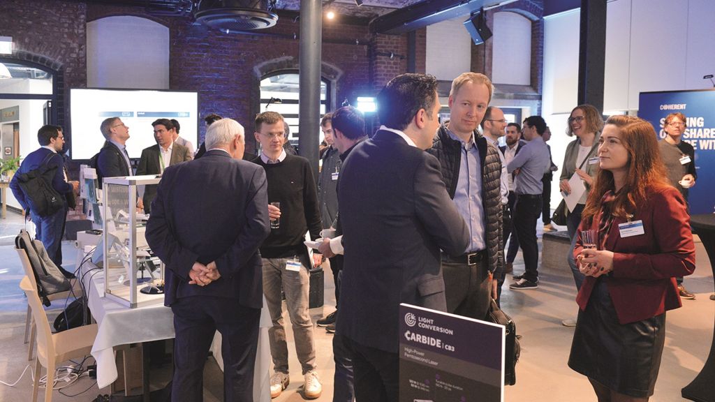
In terms of the wavelengths of laser systems, there is a trend towards ultraviolet (UV) and deep UV (DUV), with discussions focusing on advantages from the smaller focus spot as well as the ablation of transparent materials. Applications in the consumer electronics market, especially display manufacturing, are driving further development. Excimer lasers still dominate there, but solid-state UKP lasers are on the rise, as heard from Coherent.
Light Conversion provided interesting data on the performance and lifespan of various lasers at the workshop. The overview ranged from more than 10,000 hours for the 30 W UV system to just under 30 minutes in tests for generating a wavelength of 172 nanometers, corresponding to the 6th harmonic.
A new system from EKSPLA surprised attendees, providing ns and fs pulses from a single laser. The pulses are synchronized with a source, allowing users to freely adjust the duration and spacing of the pulses. 'It's like roughing and finishing on a machine,' noted one participant. The EKSPLA system also allows for very flexible programming of MHz and GHz bursts. Just a few years ago, these were still topics of fundamental lectures – now they are part of the standard for modern UKP beam sources.
As experts have gained a better understanding of the processes in materials in recent years, the focus of the workshop is now more on system technology. This year, special attention was given to the topic of beam shaping. Hamamatsu offers a new LCoS modulator (Liquid Crystal on Silicon) that can withstand powers of up to 700 watts or 3 kW/cm² thanks to the use of sapphire. Users can shape beams almost arbitrarily – ring and top-hat profiles are just two examples. They also create multi-beam profiles or correct aberrations.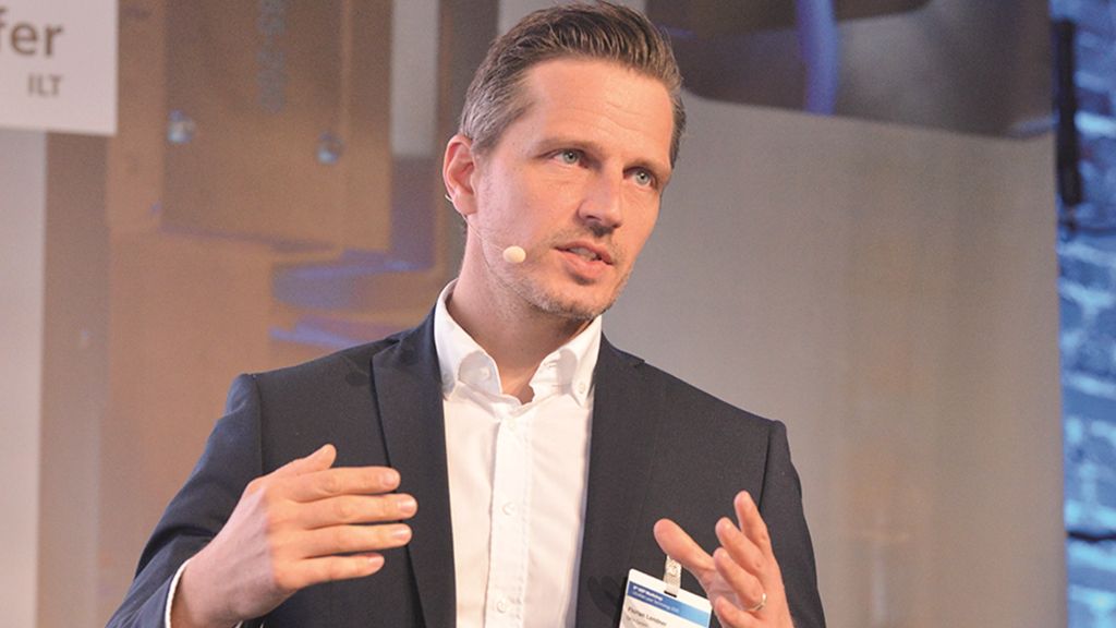
Silicon Light Machines showcased similar modulators based on micro-electromechanical systems (MEMS). They are faster (100-500 kHz refresh rate) than LCoS modulators, can handle up to 10 kW/cm², but have lower resolution. Those who do not need the flexibility of the modulators revert to diffractive optical elements (DOE), which combine high resolution with high damage thresholds. HOLO/OR presented their advantages and disadvantages in application with scanner systems.
The latter have also made significant progress. The polygon scanner from MOEWE in Mittweida achieves deflection speeds of up to 1000 m/s for the laser beam. The developers had to solve a central problem: handling the enormous data volumes of up to 38 GB per square meter of processing area, which occur during fast engraving. For printing rollers with over 100 square meters of area, they therefore relied on segmented areas. For such applications, experts expect a significant increase in productivity through the use of more powerful beam sources.
Companies like SCANLAB and AEROTECH are strategically combining scanners, acousto-optical modulators, and axis systems to leverage the strengths of each system for higher throughput. They expect that cascading the components will lead to higher duty cycles of the process, resulting in increased productivity.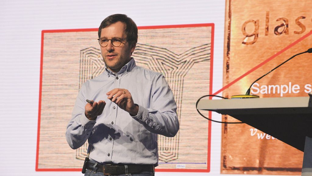
Martin Reininghaus presented another way to scale productivity with the multi-beam machines from Pulsar Photonics. For this, Pulsar has developed a multi-scanner and multi-scanner head concept alongside the multi-beam head. Multi-beam heads are suitable for highly productive manufacturing of periodic structures, while in multi-scanner setups, each scanner can operate independently. However, it is a challenge to distribute the large data volumes and laser pulses to the various scanners at the right time.
Florian Lendner from GFH demonstrated the importance of inline process control. By consistently monitoring process and environmental parameters, his team identified a long-term drift that could be compensated for by an automated correction routine. This improved the dimensional accuracy of components to ± 1 µm, further enhancing the precision of micro-processing.
Dr. Jens Ulrich Thomas (Schott AG) shared experiences in micro-welding glass. Schott has implemented the process at the wafer level and achieves connections with a shear strength of over 50 MPa. The company uses the technology in the medical technology sector. Adhesive-free joining processes reduce the approval effort there.
The company Lidrotec aims to reduce material losses in the semiconductor market with its special application of laser pulses through a liquid layer when singulating chips. Accordingly, Lidrotec is preparing the technology for large-scale applications.
Laser technology you can touch: 'The Marketplace' on campus
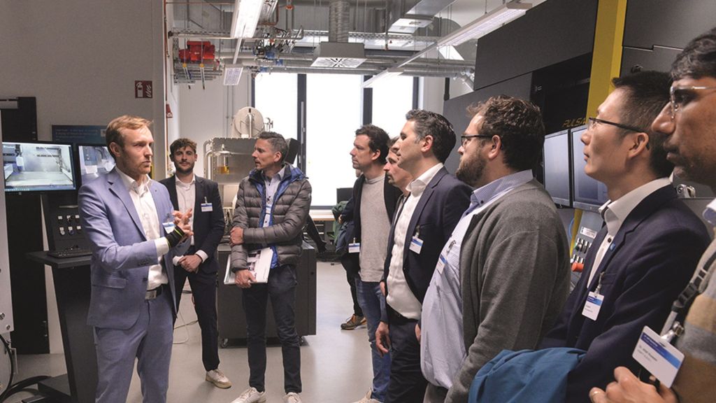
The tour through the laboratories of Fraunhofer ILT, the RWTH 'Research Campus Digital Photonic Production', and RWTH Aachen – Chair of Laser Technology and RWTH Aachen – Chair of Optical Systems Technology offered nine stations to see many of the technologies presented at the workshop live. One application presented was selective laser-induced etching (SLE). Here, the focused laser beam writes the contour of the desired component into a glass blank, which is then revealed through an etching process.
Astrid Saßmannshausen (Fraunhofer ILT) demonstrated in the lab and later in the workshop how she manufactures micro- and macro-optical components such as lenses using this process. The advantage of this method lies in the design freedom ('Complexity for free') and customizability. After the shape is created, the surface is laser-polished. The UKP laser can also directly remove material from the surface of glass, where there is always a compromise to be found between process speed and surface quality.
Many activities related to beam shaping using liquid crystal modulators were also showcased. Examples were provided earlier by Martin Kratz and Martin Osbild (both Fraunhofer ILT) regarding the SLE process and surface structuring.
Beam shaping can reduce spherical aberrations, create multi-beam profiles, or form optical stamps that can structure larger areas in one go. Paul Buske from RWTH Aachen – Chair of Optical Systems Technology demonstrated how these beam shapes can be generated as perfectly as possible using neural networks in his presentation.
Open, highly specialized, future-oriented – the UKP Workshop 2025
'It is always impressive how openly the UKP community discusses technical details here,' said Dr. Dennis Haasler, group leader at Fraunhofer ILT and chair of the workshop, at the conclusion of the 8th UKP Workshop on Ultrafast Laser Technology. 'Once again, the workshop has proven to be an excellent platform for exchange between research and development and industry,' added Dr. Christian Vedder, head of the Surface Technology Department at Fraunhofer ILT.
This year, the focus was on further scaling of manufacturing processes, for which numerous innovations, especially from the field of process technology, were discussed. The next UKP Workshop on Ultrafast Laser Technology is planned for April 28 and 29, 2027.
Contact:


